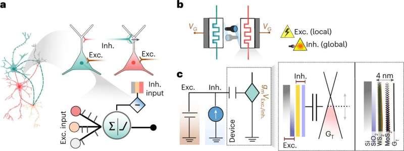
Competitive neuron concept. Credit: Nature Nanotechnology (2023). DOI: 10.1038/s41565-023-01391-6
Researchers have created atomically thin artificial neurons capable of processing both light and electric signals for computing. The material enables the simultaneous existence of separate feedforward and feedback paths within a neural network, boosting the ability to solve complex problems.
For decades, scientists have been investigating how to recreate the versatile computational capabilities of biological neurons to develop faster and more energy-efficient machine learning systems. One promising approach involves the use of memristors: electronic components capable of storing a value by modifying their conductance and then utilizing that value for in-memory processing.
However, a key challenge to replicating the complex processes of biological neurons and brains using memristors has been the difficulty in integrating both feedforward and feedback neuronal signals. These mechanisms underpin our cognitive ability to learn complex tasks, using rewards and errors.
A team of researchers at the University of Oxford, IBM Research Europe, and the University of Texas, have announced an important feat: the development of atomically thin artificial neurons created by stacking two-dimensional (2D) materials. The results have been published in Nature Nanotechnology.
In the study, the researchers expanded the functionality of the electronic memristors by making them responsive to optical as well as electrical signals. This enabled the simultaneous existence of separate feedforward and feedback paths within the network. The advancement allowed the team to create winner-take-all neural networks: computational learning programs with the potential for solving complex problems in machine learning, such as unsupervised learning in clustering and combinatorial optimization problems.
2D materials are made up of just a few layers of atoms, and this fine scale gives them various exotic properties, which can be fine-tuned depending on how the materials are layered. In this study, the researchers used a stack of three 2D materials—graphene, molybdenum disulfide and tungsten disulfide—to create a device that shows a change in its conductance depending on the power and duration of light/electricity that is shone on it.
Unlike digital storage devices, these devices are analog and operate similarly to the synapses and neurons in our biological brain. The analog feature allows for computations, where a sequence of electrical or optical signals sent to the device produces gradual changes in the amount of stored electronic charge. This process forms the basis for threshold modes for neuronal computations, analogous to the way our brain processes a combination of excitatory and inhibitory signals.
Lead author Dr. Ghazi Sarwat Syed, a Research Staff Member at IBM Research Europe Switzerland, said, "This is a highly exciting development. Our study has introduced a novel concept that surpasses the fixed feedforward operation typically utilized in current artificial neural networks. Besides the potential applications in AI hardware, these current proof-of-principle results demonstrate an important scientific advancement in the wider fields of neuromorphic engineering and algorithms, enabling us to better emulate and comprehend the brain."
Dr. Syed and Dr. Yingqiu Zhou (who were DPhil students and lab colleagues at Oxford) conducted the experimental work. According to Dr. Zhou, now a Postdoctoral researcher at Denmark Technical University, their implementation captures the essential components of a biological neuron through the optoelectronic physics of low-dimensional systems.
They note that we have created atomically abrupt semiconductor junctions through the design of our heterostructure stack. The stack, specifically delivers a heterojunction that acts as the neuronal membrane, while the graphene electrodes that contact the heterojunction serve as the neuronal soma. This way the neuronal state is represented in the soma, but modified by the changes in the membrane, just like in actual neurons.
As the advancement of artificial intelligence applications has grown exponentially, the computational power required has outpaced the development of new hardware based on traditional processors. There is an urgent need to research new techniques, including the work of co-lead author Professor Harish Bhaskaran at the Advanced Nanoscale Engineering Laboratory, University of Oxford, and at IBM Research Zurich laboratory.
Professor Bhaskaran said, "This entire field is super-exciting, as materials innovations, device innovations, and novel insights into how they can be creatively applied all need to come together. This work represents a new toolkit, exploring the power of 2D materials, not in transistors, but for novel computing paradigms."
Co-author Professor Jamie Warner, University of Texas at Austin, said, "The use of such 2D structures in computing has been spoken about for years, but only now are we finally seeing the payoff after spending over seven years in development. By assembling wafer-scale 2D monolayers into complex ultrathin optoelectronic devices, this will enable the start of new information processing approaches using 2D materials based on industrially scalable fabrication methods."
"Our findings are more of exploratory nature than actual demonstrations at the system level," Dr. Syed says. "Although we aim to expand on this concept in the future, we are convinced that our current proof-of-principle results demonstrate an important scientific interest in the wider fields of neuromorphic engineering, enabling us to better emulate and comprehend the brain."
Professor Bhaskaran points out that exciting research developments are important for future innovation, but this is not technology that one should expect in their mobile phones in the next two years.
More information: Ghazi Sarwat Syed et al, Atomically thin optomemristive feedback neurons, Nature Nanotechnology (2023). DOI: 10.1038/s41565-023-01391-6
Journal information: Nature Nanotechnology
Provided by University of Oxford


